Why Are DDR and LPDDR Incompatible with Each Other?
- 24 Jun, 2026
Are DDR and LPDDR mutually compatible during system design? For a main host SoC, how do we make the correct selection and design decisions between DDR and LPDDR? This article attempts to explain and summarize these DDR and LPDDR compatibility issues in detail.
DDR and LPDDR Are Not Directly Compatible
The DDR and LPDDR memory standards we encounter in electronic system design are targeted at completely different application scenarios.
- Standard DDR primarily targets applications such as PCs and servers, which are insensitive to power consumption but demand extreme capacity and versatility.
- LPDDR (Low Power DDR), on the other hand, is specifically designed for power- and space-constrained scenarios such as smartphones, laptops, wearables, and various edge computing devices.
Although both belong to the category of SDRAM (Synchronous Dynamic Random-Access Memory) and share similar names, in actual hardware design and component selection, DDR and LPDDR are absolutely not directly compatible or interchangeable.
Why Are DDR and LPDDR Incompatible?
The reasons for the incompatibility between DDR and LPDDR manifest in multiple aspects. These include both the electrical specifications implemented by the DDR controller and Physical Layer (PHY), as well as their internal block architectures. This has been briefly introduced in the articles Can PSRAM Be a Solution for DDR Shortages? and How Do PSRAM and LPDDR Reduce Power Consumption?.
Below is a detailed breakdown and summary of the specific reasons behind this incompatibility.
Different Electrical Voltage Levels
As summarized in the article How Do PSRAM and LPDDR Reduce Power Consumption?, LPDDR drops its standard IO operating voltage below 1V to further reduce power consumption.
- Pure Standard DDR Controller: Its internal PHY (Physical Layer) is designed for standard DDR. Taking DDR4 as an example, the default I/O voltage (VDDQ) output by the controller is 1.2V (using the POD signaling standard). This standard allows for a larger signal swing and strong driving capability to cope with parasitic capacitance and signal attenuation caused by longer PCB traces and DIMM slots. Consequently, its PCB routing requirements are relatively relaxed.
- LPDDR Chip: Taking LPDDR4X as an example, while its core voltage might be 1.1V, its I/O pins (VDDQ) for receiving data and commands are extremely delicate, with a standard operating voltage of 0.6V (using the LVSTL signaling standard). The signal voltage swing under this standard is tiny (typically only a few hundred millivolts). Such weak signals cannot drive long-distance traces. Therefore, LPDDR’s physical layer is designed for short-distance transmission, making impedance control in PCB routing extremely demanding.
Different Bus Pin Definitions
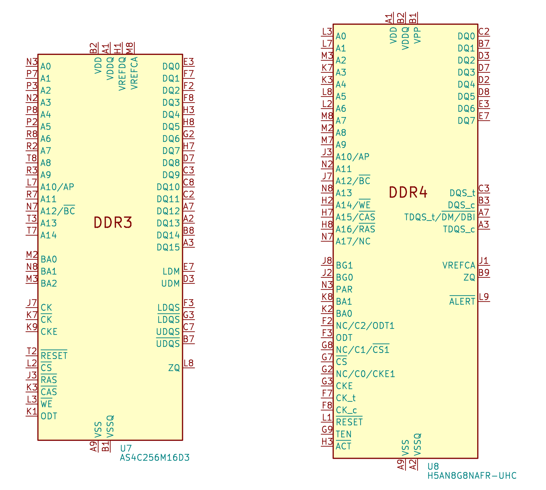
Standard DDR utilizes a split-bus design. The address lines (A0-A17), command lines (RAS, CAS, WE), and data lines (DQ) connected between the host SoC and the DDR are all separated, resulting in an extremely high pin count.
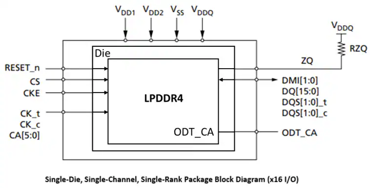
To squeeze the PCB footprint of smart devices to the absolute limit, the LPDDR standard compresses all of the aforementioned independent control and address lines into a single CA (Command/Address) bus of 10-bit (LPDDR2/3), 6-bit (LPDDR4), or 7-bit (LPDDR5). Consequently, the SoC must integrate a complex LPDDR protocol controller to split memory read/write commands and transmit them over these few CA lines across multiple cycles using both the rising and falling edges of the clock. Inside the LPDDR chip, a decoding circuit is required to reconstruct the original commands.
The figure below shows the external interface definition of DDR3/DDR4:
The figure below shows the interface definition of LPDDR4:
Different Channel Architectures
Furthermore, DDR and LPDDR exhibit fundamental differences in their underlying data transmission channel architectures.
Standard DDR typically utilizes a single 64-bit channel design (which evolved into dual 32-bit channels in DDR5), aiming to deliver massive single-transaction data throughput.
In the PC industry, PC CPU memory controllers typically operate on a 64-bit baseline. Thus, a standard DDR4 DIMM is consistently 64-bit (72-bit with ECC). In the manufacturing ecosystem of standard DDR, to control cost, package size, and yield, individual memory dies (chips) usually do not have very wide data interfaces. The most common data widths for a single chip are 4-bit, 8-bit, and 16-bit. A standard DDR controller inside a host SoC is natively designed to process 64-bit data transactions, which necessitates connecting multiple DDR chips in parallel.
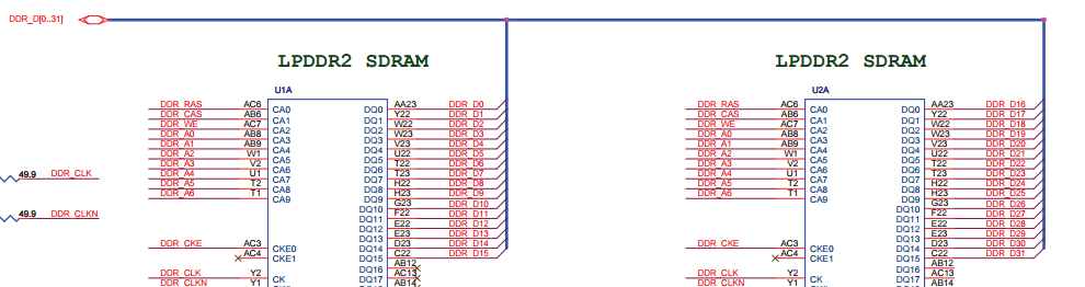
For example, if we use 8-bit memory chips, we must parallelize 8 of them to fill the 64-bit channel (8 bits/chip × 8 chips = 64 bits). During PCB routing, the SoC’s controller sends identical address and control commands (such as sharing RAS, CAS, CS) to all 8 chips simultaneously. However, the first chip is connected to the SoC’s DQ0DQ7, the second to DQ8DQ15, and so on, up to the eighth chip connected to DQ56~DQ63. When the controller issues a read command, all 8 chips output data simultaneously, forming a unified 64-bit data stream on the bus.
Of course, on consumer electronics and smart hardware mainboards, embedded applications do not require exceptionally high memory bandwidth. Since more physical pins mean larger chip packages, increased PCB layout complexity, and higher power consumption, chip manufacturers tailor their SoC designs to the application’s actual bandwidth needs. Instead of directly adopting the 64-bit data width common in PCs, they more frequently use 32-bit or even 16-bit widths.
LPDDR, conversely, adopts a completely different design architecture for its data transmission channels. To maintain high bandwidth under low power consumption, it employs a multi-channel, narrow-width architecture. For example, a single LPDDR4 chip typically consists of two independent 16-bit channels (32-bit total). As shown in the figure below, the interior of an LPDDR4 chip is split into two completely separate channels. This allows the memory controller, within the same clock cycle, to have Channel A respond to an NPU read request while Channel B responds to a CPU write request, achieving superior concurrency.
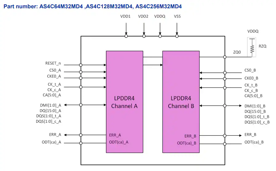
This architecture allows the SoC to schedule memory more flexibly, reducing the power overhead associated with waking up the entire memory chip. For instance, if the current system load is light, the SoC can put Channel B into a deep sleep state (such as Self-Refresh or Power Down) while keeping only Channel A active.
LPDDR Initialization Timing Issues
As summarized in the article How Do PSRAM and LPDDR Reduce Power Consumption?, LPDDR eliminates the internal DLL (Delay-Locked Loop) module to save power. To resolve high-frequency clock signal alignment issues without an internal DLL, it requires the host SoC’s memory controller to perform active phase measurement and compensation via software algorithms inside the SoC’s LPDDR controller during system boot.
- For a pure DDR controller: The controller assumes the target memory chip has an internal DLL. Thus, after sending basic reset and Mode Register Set (MRS) configurations during the bootloader stage, it naturally assumes that clock alignment has been established inside the DDR chip and immediately begins high-speed data transceiver operations.
- For LPDDR: Because LPDDR lacks an internal DLL, every time it powers up, it must wait for the SoC’s LPDDR controller to execute a complex Link Training algorithm. The SoC must actively probe the clock signal propagation delay and apply phase compensation.
A pure DDR controller does not implement these complex Link Training algorithms at all (since standard DDR does not require them). Consequently, if you connect an LPDDR chip to a standard DDR controller, the handshake phase will fail, and the system will hang during the memory initialization phase.
Different Power Delivery Networks and Power Management Mechanisms
DDR and LPDDR are completely incompatible in terms of hardware Power Tree design.
Standard DDR typically requires fewer power rails (e.g., VDD, VPP). LPDDR, for aggressive power savings, generally requires multiple low-voltage rails (e.g., VDD1, VDD2, VDDQ), and these voltages are usually significantly lower than those of contemporary standard DDR.
To achieve highly granular power management, the LPDDR specification integrates extremely complex internal power state machines. It supports advanced low-power features such as Deep Power Down and Partial Array Self-Refresh (PASR). These features require the SoC to control them via specific protocols, which standard DDR does not support.
Why Do Some SoCs Support Both DDR and LPDDR?
Based on the differences between DDR and LPDDR summarized across these various dimensions, we can conclude that the two are indeed mutually exclusive and entirely non-interchangeable. However, we do see in some SoC datasheets (such as the Rockchip processors shown below) that they can support both DDR and LPDDR memory chips. Why is this the case?
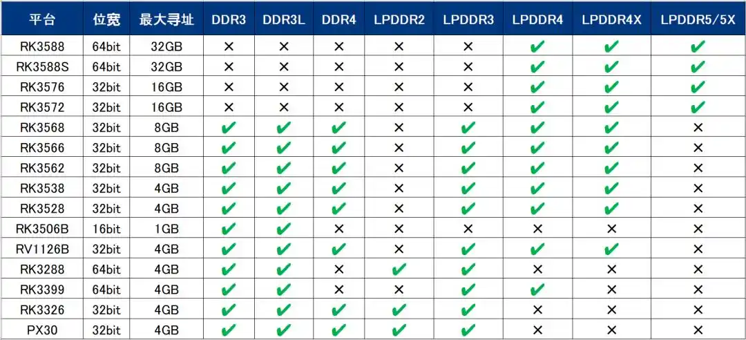
This is because chip manufacturers, in order to support a wider selection of memory components for diverse industry applications, integrate expensive and complex Combo DDR Controllers & PHYs (compatible memory controllers and physical layers) inside the SoC.
To enable a single SoC to support both DDR and LPDDR—which have vastly different physical characteristics—the internal Combo design must implement specialized logic in at least three key areas:
- Logical Control Layer: The DDR memory controller inside the SoC is no longer hard-wired. Instead, it contains two complete protocol state machines, allowing it to be configured for either DDR or LPDDR modes.
- Physical Interface Layer (PHY): To accommodate two completely different electrical standards, the I/O pads behind the external data (DQ) and control pins on the SoC must be designed with highly complex combinational circuitry. They must integrate both high-voltage, high-drive transistors for standard DDR (corresponding to SSTL signaling, such as 1.2V) and low-voltage, micro-drive transistors for LPDDR (corresponding to LVSTL signaling, such as 0.6V).
- Pin Mapping: Since their pin definitions are entirely different, the SoC utilizes a pin “superset” alongside internal multiplexing (MUX) to route connections to external DDR or LPDDR chips using the same physical pins. The SoC’s package provides a pin count matching the more demanding standard (usually standard DDR) while using internal multiplexers to remap the functionality of specific pins (such as the CA bus) based on the active mode.
It is worth noting that while an SoC’s memory subsystem can support both DDR and LPDDR through these methods, in actual product design, once the memory chip selection is finalized, the Combo PHY and PCB layout must commit exclusively to either DDR or LPDDR. Therefore, if LPDDR4 is selected during the schematic design phase, unused pins must be left floating, the motherboard’s power tree must be designed to supply multi-rail power (e.g., 1.1V/0.6V), and the BootROM configuration pins must be strapped high or low to set the host’s DDR controller to LPDDR4 mode. Once the physical hardware is manufactured, it is absolutely impossible to switch back to DDR4 via a software or firmware update.