Overview of the Working Principles of Hardware Security Chips in Embedded Products
- 06 Aug, 2024
Basically, the application of hardware security chips in embedded products mainly includes the following two categories:
- Basic anti-cloning (anti-copying) applications.
- Advanced encryption/decryption and hardware authentication applications.
This article briefly introduces the complete working principle and workflow of the former, while dedicating most of the content to the study and summary of the latter—namely, the more advanced encryption, decryption, and authentication-type security chips.
Working Workflow and Principles of Anti-Cloning Security Chips
For simple anti-cloning applications, there are many chip options available on the market, with domestic Chinese options accounting for a large portion, ranging in price from a few cents to a few dollars. The primary function they provide is adding an anti-cloning security chip to a relatively simple product to prevent unauthorized copying of both the hardware and software.
This type of product application mainly involves adding an I2C, serial (UART), or SPI-interfaced security chip to the hardware design. When the system SoC software is running, the SoC communicates with this security chip through these interfaces to exchange data. The SoC’s software logic detects the presence of the security chip and verifies the correctness of the programmed key. The system SoC will only run normally if the verification process between itself and the security chip succeeds; otherwise, it will shut down directly.
Since the key programmed inside the security chip cannot be extracted, even if someone successfully clones the hardware board and fully reads out the firmware image from the flash to write it onto their cloned board, the system SoC will fail to initialize or run properly during boot-up due to the lack of the security chip. This provides robust protection for the product’s hardware and software.
In essence, this type of anti-cloning security chip is simply a basic IC containing a cryptographic algorithm and a key storage area. The encryption algorithm is typically a shared-key symmetric algorithm, such as AES. The encryption key used by the algorithm matches the key used in the firmware validation process. Once written to the security chip, the key can neither be read nor modified. The verification algorithms on both the security chip and the firmware use the same key to encrypt a randomly generated string during each boot-up, then compare the results, thereby verifying the presence of the security chip and the correctness of the key written inside it.
Generally, the workflow of these anti-cloning security chips is as follows:
- First, during the manufacturing process, a key must be written to the security chip. This key is shared between the security chip and the firmware code. Note: Once the key is written to the security chip, it cannot be changed. Therefore, this step is critical; if the wrong key is written, the chip will be scrapped.
- The main controller (SoC) generates a random code, usually a dynamic random code based on current time information.
- The main controller sends the plaintext of the random code to the security chip via the communication interface.
- The security chip uses its internal hardware cryptographic engine and the pre-programmed production key to encrypt the plaintext random code, producing ciphertext.
- The security chip returns the ciphertext to the main controller.
- The main controller decrypts the ciphertext returned by the security chip using the decryption library provided by the chip vendor and its own production key, producing the decrypted plaintext.
- The main controller compares the decrypted plaintext with the original random code. If the values match, the authentication succeeds; if they do not match, the system shuts down.
To support these operations, security chip vendors typically need to provide:
- Blank (unprogrammed) security chips and their reference designs.
- Firmware-side cryptographic algorithm libraries. (If standard cryptographic algorithms are used, these might not be necessary, and open-source implementations can be used directly.)
- A programmer for the security chip keys. Alternatively, security chips can be designed with one-time-programmable (OTP) I2C instruction sequences, allowing factory production software to write the key during production, eliminating the need for a dedicated programmer.
Advanced Security Chips
These advanced security chips, beyond supporting basic anti-cloning functions, provide comprehensive cryptographic algorithms, key/certificate management, hardware random number generators (TRNG/PRNG), Secure Boot, and other features, offering hardware-level support for implementing robust security protection on the embedded SoC side.
Taking Microchip’s ATECC608 as an example, this widely used secure element solution provides the following features:
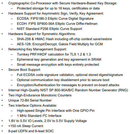
In summary:
- Key storage area, capable of storing up to 16 independent keys, certificates, and other data requiring encryption.
- Coordinates with SoC software interfaces and execution flows to implement asymmetric cryptography, authentication, ephemeral key management, and even full TLS functionality.
- Hardware cryptographic algorithms: AES128, SHA256, etc.
- Secure Boot support.
- Hardware random number generator (RNG).
First, we must clarify a fundamental question: why do we need to protect our embedded products with this dedicated hardware? Many people might assume that if we use highly secure international standard algorithms like AES, RSA, or ECC in our embedded software to protect our communications and data, the security strength is already sufficient. Moreover, many modern SoCs have built-in hardware acceleration for AES encryption/decryption, so running these standard cryptographic algorithms directly on a relatively powerful processor does not bottleneck the system. What, then, is the point of adding extra cost to use a standalone security chip?
The reason is that regardless of whether our embedded products use symmetric encryption or public-key cryptography, how these keys are stored remains the biggest challenge in system security design. Algorithms like AES and RSA are robust, but the shared keys, public/private key pairs, and certificates used with them must be saved in a secure location to make the product’s security design bulletproof. Without a dedicated hardware security chip, most system designs store this sensitive information in Flash memory, often using custom software encryption. This actually poses a massive security risk. Attackers can desolder the flash chip, read out the stored sensitive data (such as shared keys or private key certificates), and easily decrypt the device’s communications. This is why a well-secured system needs an additional, independent hardware security chip: it stores all sensitive information inside a tamper-proof hardware element that cannot be easily read or cracked. Furthermore, cryptographic operations are executed entirely within this independent hardware. Only encrypted ciphertext is transmitted between the security chip and the system SoC, making arbitrary reverse-engineering or hacking nearly impossible.
Consequently, using advanced security chips to protect sensitive information in embedded devices has increasingly become a standard feature for IoT products, and is highly recommended by major IoT cloud platform providers like Google, Amazon, and Microsoft. When an IoT product connects to these cloud platforms, a unique public/private key pair is typically generated for each device. This key pair should be written to the IoT product’s independent hardware security chip for secure storage. Subsequent encrypted communications are handled directly between the hardware security chip and the IoT Cloud, which both simplifies the system’s security architecture and significantly elevates the overall security strength of the design.
Of course, introducing additional security hardware inevitably increases the system’s BOM (Bill of Materials) cost and the workload of hardware and software development and debugging. However, whether to include it ultimately depends on the security requirements of the specific product.
Application Logic of ATECC608A in Products
Note: Due to a lack of test hardware on hand, the following information is summarized from online resources and study. It may contain inaccuracies and is intended for reference at the system design level only.
When discussing advanced security chips widely used in embedded products today, Microchip’s ATECC608 series is almost impossible to ignore. In fact, some domestic Chinese chip manufacturers have created pin-to-pin compatible alternatives (such as the Mod8ID) that can even directly reuse the cryptoauthlib software library, significantly reducing the difficulty and workload of migrating from the ATECC608.
Therefore, taking ATECC608 as an example, understanding the application logic of these advanced security chips in embedded development will provide a systematic and comprehensive understanding of how to use them to deliver robust security protection in product designs.
To support development with the ATECC series, Microchip maintains a cross-platform C library on GitHub called cryptoauthlib (link: https://github.com/MicrochipTech/cryptoauthlib). Whether developing software for an embedded MCU or an embedded Linux system, direct access to the hardware security chip ultimately relies on this library.
Configuring the Security Chip
Similar to the anti-cloning security chips discussed earlier, before actually using the security chip for security protection in your application logic, you must first write the configuration settings and sensitive data (such as various keys, certificates, and other confidential data) according to your application requirements and then “lock” the chip. Once the configuration zone is written and locked, the settings cannot be modified, so extreme caution is required during debugging.
Writing the internal configuration and security data for the ATECC608 is also accomplished by calling APIs from the cryptoauthlib library.
The internal data storage of ATECC608 consists of two parts: the Config Zone and the Data Zone.
- The Config Zone is a fixed 128-byte area, with the first 16 bytes being read-only. The data in this zone is primarily used to define how the data in each slot of the Data Zone is accessed and secured. Because understanding the configuration settings can be relatively complex, it is recommended to modify the official configuration templates provided by Microchip according to your needs to avoid errors.
- The Data Zone contains 16 slots. Each slot can store security-related information as defined by the corresponding configuration in the Config Zone. The types of data stored in each slot vary; for example, Slot 9 is commonly used to store an AES key.
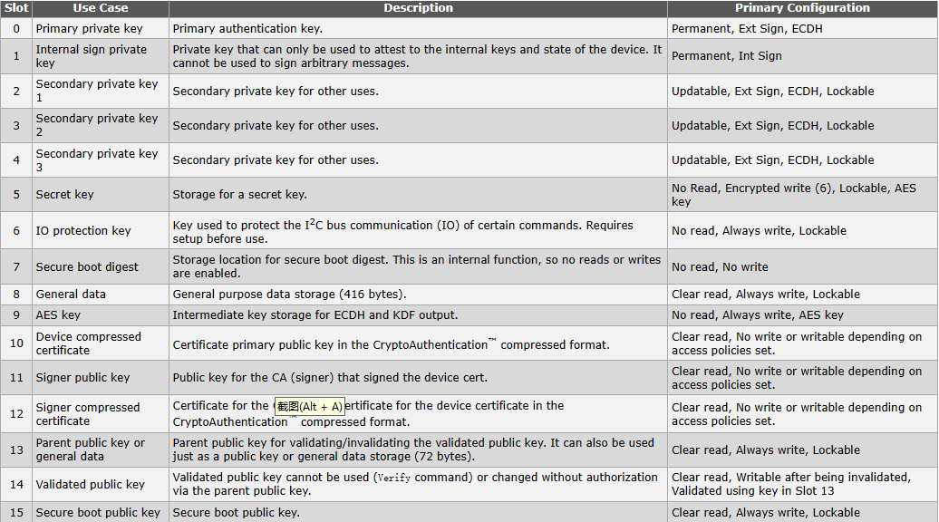
Once the Config Zone and Data Zone details are finalized, you can call the atcab_write_bytes_zone or atcab_write_zone functions from the cryptoauthlib library to write them to the security chip. After writing this information and locking the zones (locking is typically performed by calling APIs such as atcab_lock_config_zone and atcab_lock_data_zone in cryptoauthlib), the security chip hardware is ready for use.
Programming the configuration and security data should be done during the factory testing/production phase before the product leaves the factory, by invoking the appropriate APIs in cryptoauthlib.
Application Logic of ATECC608 in Embedded MCU Products
Reference Document 3 provides a hardware security design using ATECC608 on the Arduino platform. Below is a summary of the study notes for that document.
Reference Document 3 includes an example of using the security chip for AES encryption. The prerequisite for performing AES encryption is that the AES key has already been written and the chip locked in the previous "
Performing AES encryption on the MCU is then relatively straightforward. The general workflow is as follows:
- Initialization: Call
atcab_init(ATCAIfaceCfg *cfg)to initialize. - Initialize AES settings: Call
atcab_aes_cbc_init(atca_aes_cbc_ctx_t* ctx, uint16_t key_id, uint8_t key_block, const uint8_t* iv)to select which slot contains the AES key to use (specified bykey_id), which 16-byte block in that slot is the key (specified bykey_block), and the initialization vector (iv) required for execution. - AES-128 Encryption: Call
atcab_aes_cbc_encrypt_block(atca_aes_cbc_ctx_t* ctx, const uint8_t* plaintext, uint8_t* ciphertext)to perform AES-128 encryption. Since ATECC608 only supports 128-bit AES block encryption, the input plaintext passed in each call is fixed at 16 bytes, and the output ciphertext is also fixed at 16 bytes. If the data to be encrypted exceeds 16 bytes, you must manually split it into multiple calls at the application layer. - AES-128 Decryption: Call
atcab_aes_cbc_decrypt_block(atca_aes_cbc_ctx_t* ctx, const uint8_t* ciphertext, uint8_t* plaintext)to perform AES-128 decryption. The parameters passed are identical to encryption, with processing restricted to fixed 16-byte blocks.
The complete AES encryption/decryption workflow is executed entirely inside the ATECC608 hardware. Plaintext is sent in via I2C, and ciphertext is read out via I2C; the decryption process follows the same logic. With both the encryption algorithm and the key residing inside the hardware security chip, the overall product security is exceptionally robust.
Of course, to run this workflow on an embedded MCU, you must first port the cryptoauthlib library to your MCU hardware. Fortunately, cryptoauthlib is cross-platform, pure C code, and there are numerous existing porting examples for various MCUs on the market. For specific porting instructions, refer to the official documentation and online search resources.
Application Logic of ATECC608 in Embedded Linux Products
Reference Documents 4 and 5 provide a system hardware security design using ATECC608 on the Raspberry Pi and Linux platform. Below is a summary of the study notes for those documents.
Using the ATECC security solution on an embedded Linux system involves an entirely different operational logic compared to an embedded MCU. Instead of directly calling the cryptographic interfaces of cryptoauthlib, these hardware security solutions on embedded Linux are typically used in conjunction with standard software security solutions like OpenSSL. The ATECC chip provides hardware-accelerated cryptographic operations, key management and storage, and random number generation directly to OpenSSL.
As mentioned earlier, without a hardware security chip, using OpenSSL for secure communications inevitably requires saving private keys, certificates, and shared keys within the filesystem on Flash storage. This risk is the greatest vulnerability of pure software security solutions. Using a dedicated hardware solution like the ATECC series provides a secure, convenient hardware foundation for OpenSSL. Sensitive information like keys is no longer stored in Flash, but directly inside the security chip. Once compiled and configured, the security chip serves as a secure hardware backend for OpenSSL, while the user-space applications continue to interact with OpenSSL. This security architecture is transparent to the application layer. Whether using software or hardware encryption, or switching to different security chip vendors, as long as it is configured to work with OpenSSL, the application-layer code requires zero modification. This seamless integration makes this model highly popular among product developers.
The standard interface between OpenSSL and hardware security chips described above is PKCS#11. Fortunately, Microchip designed cryptoauthlib with this in mind, making it easy to implement the PKCS#11 interface for seamless communication with OpenSSL and other libraries. With appropriate configuration and cross-compilation, cryptoauthlib can act as a standard PKCS#11 provider.
The general workflow for using the ATECC608 on an embedded Linux platform is as follows:
- Cross-compile the
cryptoauthliblibrary, enabling compilation options likeATCA_OPENSSLandATCA_PKCS11. This generates the shared librarylibcryptoauth.so, which should be installed under/usr/lib/. - Cross-compile and install the
libp11third-party library. - Modify the configuration file of the
cryptoauthliblibrary, located at/var/lib/cryptoauthlib/<slot number>.conf. In this configuration file, define the I2C device address of the ATECC608 chip, as well as the slot locations for various security assets (i.e., the slot numbers where the private key, certificate, public key, etc., are stored). - Use the
p11toolfrom thegnutls-binpackage to attempt communication withlibcryptoauth.soand the hardware security chip to verify if the current configuration is correct:- $ p11tool —provider /usr/lib/libcryptoauthlib.so —list-all
- Modify the OpenSSL configuration file
openssl.cnfto use the PKCS#11 interface (by specifying the path tolibpkcs11.sogenerated during the compilation oflibp11earlier) and configure its PKCS#11 provider to point tolibcryptoauth.so. - This completes the integrated configuration of OpenSSL, PKCS#11, and
cryptoauthlib. Subsequent OpenSSL operations can now interact directly with the hardware security chip. You can then use the OpenSSL command-line tool to generate keys or perform mutual TLS authentication tests. At this point, any OpenSSL-based application will function normally.
References:
- Principles and Selection of Security Chips - LCSC (szlcsc.com)
- Introduction to Hardware Security Chips, Selection, and Working Principles - Tencent Cloud Developer Community (tencent.com)
- Security With Arduino : Atecc608a : 7 Steps - Instructables
- https://kickstartembedded.com/2022/03/25/raspberry-pi-atecc608-part-1-overcoming-modern-iot-security-challenges/
- Raspberry Pi + ATECC608: Part 2 – About PKCS#11 and Testing Mutual TLS Authentication – Kickstart Embedded