A Beginner's Guide to NFC Technology
- 22 Jun, 2026
NFC (Near Field Communication) is a high-frequency RFID (Radio Frequency Identification) technology widely used in today’s consumer electronics. This article provides a comprehensive summary of the foundational theory and application knowledge associated with this technology, helping to establish a basic understanding of NFC.
NFC Technology Basics and Comparison with RFID
NFC technical specifications operate in the globally unlicensed 13.56 MHz frequency band. Unlike Bluetooth or Wi-Fi, which communicate by actively emitting electromagnetic waves (far-field radiation), NFC relies on inductive coupling (near-field principle) to exchange information.
Inductive coupling can be thought of as an air-core transformer. During communication, the antenna coil of the reader (initiator/master device) generates an alternating magnetic field. When a tag (target/slave device) is brought close, its antenna coil induces a current. This process not only transmits data but can also supply power to passive tags.
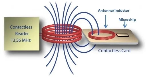
Looking solely at the working principle of inductive coupling, one might find that NFC technology is virtually identical to ordinary RFID as well as the communication technologies used in automotive keyless systems like RKE/PEPS. So, specifically, what makes NFC unique in its applications?
The following table compares the technical specifications and application fields of these three technologies:
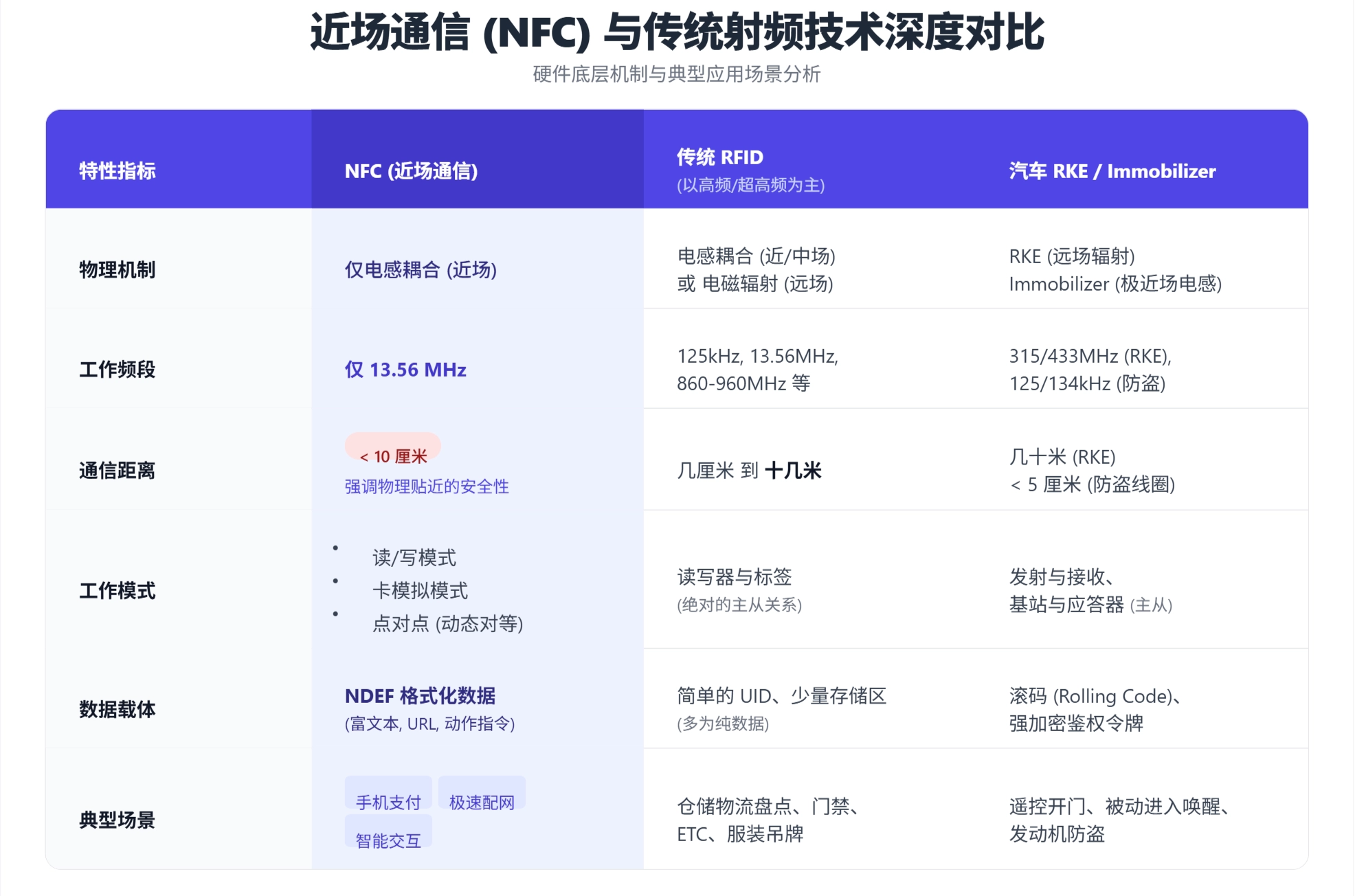
Specifically, the main differences are:
- NFC operates exclusively in the 13.56 MHz band, whereas the other two have multiple frequency bands available.
- NFC is designed for a communication distance of less than 10 cm (in actual products, this is typically restricted to 1–3 cm to pass certifications). This extremely short range serves as an intentional physical security barrier, ensuring that every data exchange requires a deliberate, subjective physical touch (“Tap”) by the user, thereby preventing malicious long-range eavesdropping. In contrast, traditional RFID and automotive PEPS systems generally have communication ranges of dozens of meters.
- NFC offers more flexible operating modes, supporting three distinct operating modes and role-switching during communication. Traditional RFID and automotive PEPS systems, on the other hand, maintain a static relationship between a fixed reader and tag (i.e., transmitter and receiver).
- The core value of NFC lies in its ability to transmit rich text data, whereas the tags in the other two technologies typically only store a very simple UID (Unique Identifier) or a few encrypted keys used solely for identity verification.
NFC System Architecture and Operating Modes
In PCB-level designs for consumer electronics, a complete NFC RF front-end system typically comprises the following three core components:
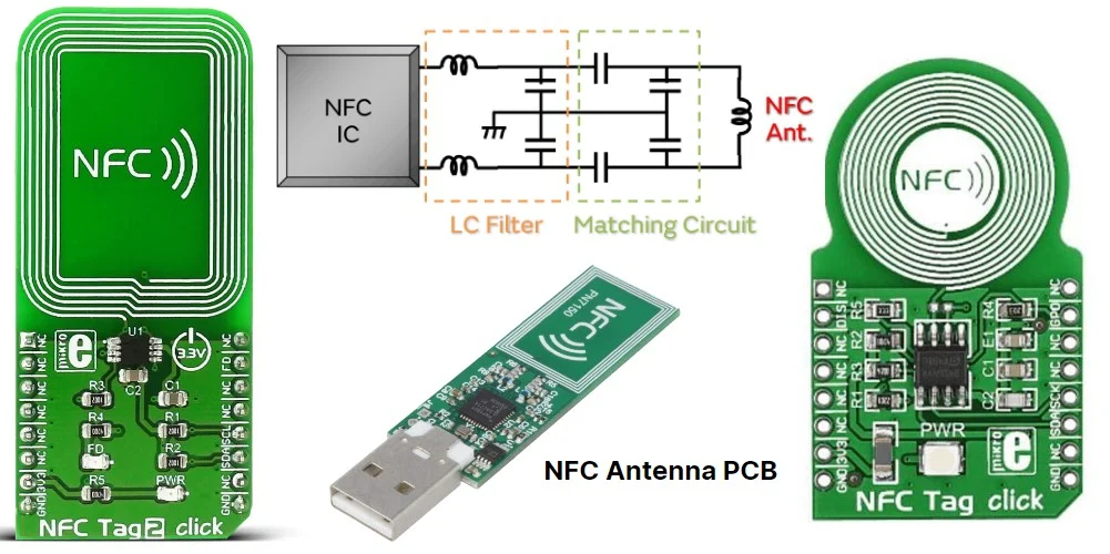
- NFC Controller (NFC Controller IC): This integrates an RF transceiver, modem, and protocol-processing microcontroller. The controller module typically communicates with the host controller (MCU/SoC) via an I2C or SPI interface. High-end NFC controllers feature built-in firmware that directly outputs the standard NCI (NFC Controller Interface) instruction set, significantly easing the burden of low-level driver development on the host.
- EMC Filter and Antenna Matching Network: The signals output by NFC chips are square waves containing many harmonics. Therefore, during hardware debugging, an LC filter circuit (to filter out interference outside 13.56 MHz) and an impedance-matching network must be designed between the chip’s Tx/Rx pins and the antenna. This ensures conjugate matching between the chip’s output impedance and the antenna’s impedance, achieving maximum power transfer efficiency.
- NFC Antenna: This is usually an inductive coil with a few turns. In consumer electronics, the antenna can be a PCB trace (lowest cost but occupies a large area), an FPC (flexible printed circuit, often adhered to the inside of the device housing), or a customized ferrite-backed wire-wound antenna (suitable for metal environments).
Modern full-featured NFC chips (such as the PN7160 or ST25R3916) feature a symmetric internal RF architecture, meaning they contain both transmission (Tx) and reception (Rx) paths. During communication, the chip uses low-level switch matrices and state machines to dynamically assume initiator (master) or target (slave) roles.
The RF pins of these full-featured NFC chips typically interface with two sets of RF paths:
- Tx Path (Transmitter): This contains an internal Power Amplifier (PA) powered by VDD_PA. Its job is to drive the external LC resonant antenna, radiating an alternating 13.56 MHz magnetic field.
- Rx Path (Receiver): This includes a highly sensitive detector and demodulator inside, responsible for monitoring minute voltage amplitude changes or phase shifts on the antenna.
Thus, if the NFC chip in a product is a full-featured chip, it means its physical RF architecture is complete, capable of both transmitting (generating a field) and receiving (sensing a field). Conversely, passive NFC tags (such as consumable stickers) have a pared-down hardware architecture. They lack an internally powered Tx PA, containing only an antenna coil, a rectifier circuit (to harvest power from the magnetic field), and an electronic switch to modulate their own impedance—essentially having only Rx capabilities.
The Three Communication Modes of NFC
In system development, NFC supports three standard operating modes:
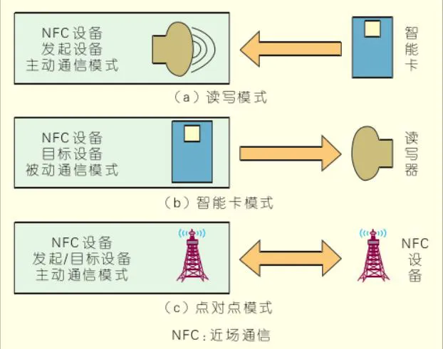
- Reader/Writer Mode: The most common mode. The device actively generates a magnetic field to read from or write to a passive NFC tag or smart card. In this mode, the local device’s NFC chip enables its internal PA, continuously pumping energy through the Tx pin to the antenna to generate a stable 13.56 MHz magnetic field. Throughout the subsequent communication, even when reading data, the device must maintain an active Tx magnetic field.
- Card Emulation Mode: The device behaves like a standard contactless smart card (such as an access card, transit card, or bank card), with the magnetic field provided by an external reader (such as a turnstile). In this mode, the device’s NFC chip completely turns off its Tx PA and no longer radiates energy, saving power. The turnstile’s magnetic field induces a voltage on the card device’s antenna. The energy harvesting pin (or a dedicated wake-up pin) on the NFC chip detects this field and wakes up the host controller.
- Peer-to-Peer (P2P) Mode: Two active NFC devices establish a bidirectional communication channel to exchange data when brought close to each other. (Note that in modern consumer hardware, this mode is rarely used as the primary data transfer channel; it is mostly used for handshaking, such as bootstrapping a Wi-Fi connection). Both devices are full-featured NFC devices. When they get close, they negotiate their roles for subsequent communication through a handshake, establishing one as the Initiator and the other as the Target.
The next question arises: Given that the RF link design of full-featured NFC is symmetric and supports these three operating modes, how does a full-featured NFC device actively or passively choose which mode and role to operate in during runtime?
The answer is: It relies on the NFC Discovery Loop and active configuration intervention by the host controller (MCU).
For a full-featured NFC controller whose mode is not restricted by the host controller (MCU), it automatically runs a time-division-multiplexed state machine at the physical layer upon powering up into standby. This state machine is called the Discovery Loop.
The basic operational logic is that this state machine switches frequently among three states: Poll, Listen, and Sleep—typically with a full cycle lasting a few hundred milliseconds. If it detects a passive tag while in the Poll state during this transition, it operates in Reader/Writer mode. If it detects an external reader/turnstile, it operates in Card Emulation mode.
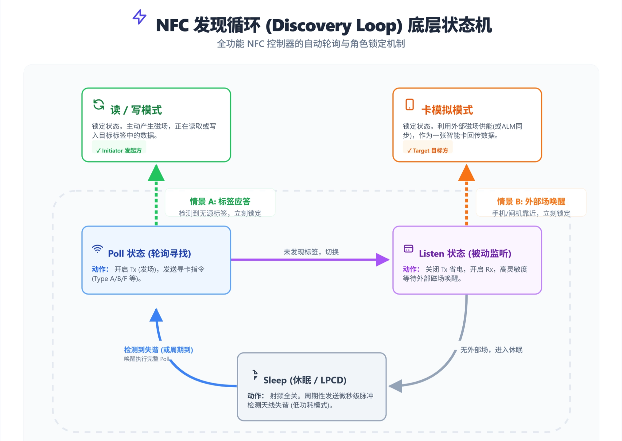
In practical product development, leaving all modes enabled to loop indefinitely is both power-inefficient and prone to unnecessary interaction conflicts. Usually, the application scenario for a product’s NFC functionality is clear and predefined. Therefore, during system implementation, the host MCU’s application should actively configure the routing table and discovery rules during system initialization based on business logic requirements, instead of letting the chip poll inefficiently in the background without restriction.
- If the primary use case of the product’s NFC functionality is to read passive NFC tags and there is no need for it to be read as a card by phones or turnstiles, the MCU can send NCI commands to the NFC chip to disable the Listen State and P2P mode. Consequently, the chip’s Discovery Loop will only contain Poll and Sleep, turning it into a pure active reader/writer.
- If the product’s use case requires it to act both as a reader (reading a user’s physical access card) and as a card (allowing a phone with NFC card-emulation to tap and open a door), then the complete Discovery Loop must be preserved.
Regardless, in battery-powered electronic products, to achieve extreme power savings, the Poll state is typically replaced by LPCD (Low Power Card Detection).
In the LPCD state, the device’s transmitter (Tx) no longer sends full protocol packets. Instead, it emits an extremely short pulse field every few hundred milliseconds to detect whether the antenna’s inductance has shifted slightly (since metal or an approaching card causes antenna detuning). If detuning is detected, the chip fully wakes up to execute the complete Poll process. Consequently, the chip only powers up to generate a full RF field when someone actually taps a card against the antenna, reducing standby power consumption from tens of milliamperes to the microampere range.
What is the NCI Instruction Set?
As mentioned above, some high-end NFC controllers run internal firmware that supports the standard NCI (NFC Controller Interface) instruction set. When configuring the NFC operating modes, the host MCU interacts with the NFC chip by sending NCI commands over hardware interfaces like I2C or SPI. So, what exactly is this NCI instruction set?
Before the standardization of the NCI (NFC Controller Interface) instruction set, the low-level registers and control logic of different NFC chip manufacturers varied wildly. If software engineers wanted to switch to a different NFC chip, they had to rewrite almost the entire driver layer. To address this, the NFC Forum established the NCI standard, with the goal of completely abstracting away the complexities of low-level RF timing and physical links.
Empowered by the NCI instruction set, the host processor only needs to send standardized NCI byte streams to the NFC chip via I2C or SPI. The chip then automatically handles complex tasks like RF wake-up, collision detection, and low-level protocol validation. Consequently, if you need to switch the NFC chip during product development, you only need to swap in another chip that supports the same NCI instruction set. The driver and application layers on the host side require virtually no changes. (Of course, in reality, things are rarely so ideal, as some manufacturers append proprietary custom commands to the NCI framework, requiring extra debugging.)
The NCI specification strictly classifies packets transmitted over physical buses (such as I2C or SPI) into four types:
- CMD (Command): Host (MCU/SoC) $\rightarrow$ NFC chip. These are action instructions issued by the host.
- RSP (Response): NFC chip $\rightarrow$ Host. A synchronous response to a CMD. The chip must reply with an RSP within a very short time after receiving a CMD.
- NTF (Notification): NFC chip $\rightarrow$ Host. Asynchronous events actively reported by the chip.
- DATA: Bidirectional. Pure payload pass-through for the application layer. Once a low-level connection is established, the actual data read from or written to the card/external device (such as NDEF rich text or URLs) is encapsulated in DATA packets.
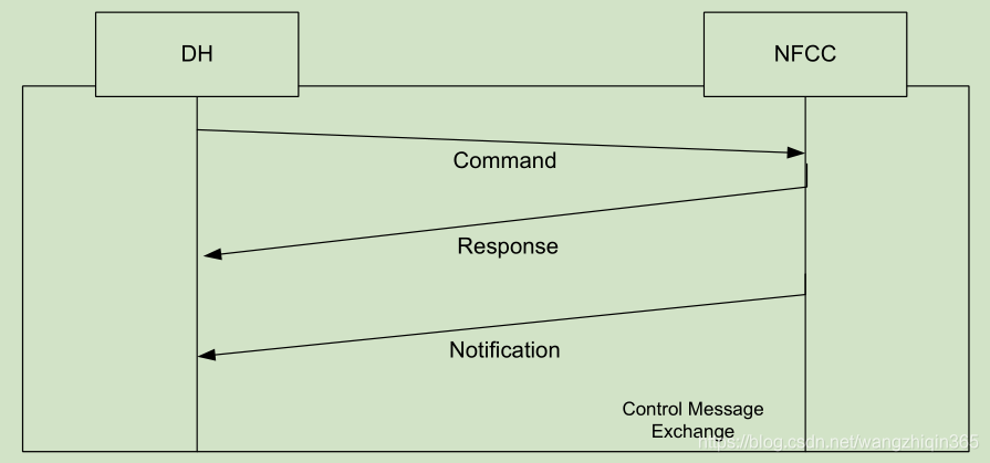
During the software development phase, the standardization of NCI offers immense convenience for team division of labor:
- BSP / Driver Layer: Driver engineers do not need to understand any of the NFC protocol stack logic. They only need to bring up the I2C or SPI interface in Linux/RTOS and configure a GPIO interrupt pin (used to trigger an interrupt when the NFC chip sends an NTF notification to the host). In Linux, this typically manifests as a simple character device node (e.g.,
/dev/pn544or a device registered via the I2C core layer). The sole purpose of this node is the transparent transmission of NCI byte streams. - Protocol Stack (Middleware): The parsing and assembly of NCI packets are handled by middleware. For instance, NXP provides the Linux-based
libnfc-ncilibrary. For Android systems, the AOSP source tree built-insystem/nfcalready contains a highly mature and comprehensive NCI protocol stack. - Linux Application Layer / Apps: Application developers can directly call high-level APIs exposed by the protocol stack/middleware, such as
nfc_enable(),nfc_read_ndef(), and so on.
MIFARE / FeliCa / ISO/IEC 14443
Before NFC standards were established, various semiconductor giants in the 13.56 MHz high-frequency RFID space proposed their own low-level modulation schemes and proprietary data formats. When the NFC Forum was later founded, its brilliance lay not in inventing a brand-new RF technology, but in offering backward compatibility with these proprietary solutions while unifying them at the higher layer into the standardized NDEF (NFC Data Exchange Format) data format.
Within this domain, NFC provides backward-compatible support for five major technical streams:
- MIFARE: Led by NXP, this is currently the world’s most widely adopted contactless smart card technology. Its physical layer is primarily based on the ISO/IEC 14443 Type A RF standard. It is incredibly ubiquitous, used in residential access control cards, hotel key cards, transit cards, and disposable paper tickets/stickers.
- FeliCa: A proprietary standard developed by Sony, corresponding to the Japanese Industrial Standard JIS X 6319-4. It is the dominant standard in Japan’s Suica (watermelon card) and Hong Kong’s Octopus card systems.
- ISO/IEC 14443 Type B: During the creation of the 14443 standard, NXP championed Type A, whereas STMicroelectronics (ST), Motorola, and others jointly backed Type B, which is better suited for high-density cryptographic operations. China’s second-generation resident ID cards, various contact/contactless bank cards (EMV standard), and e-passports almost exclusively adopt the Type B standard.
- ISO/IEC 15693: Compared to the aforementioned technologies, this standard sacrifices communication speed to achieve a longer read/write range (up to dozens of centimeters) and supports rapid, simultaneous anti-collision reading of multiple tags. Typical applications include library self-checkout systems, contactless ski passes, and batch inventory of medical reagent kits.
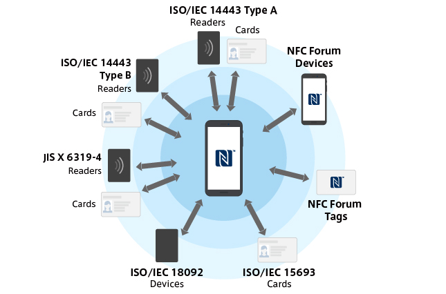
Facing such a diverse array of underlying chips for contactless cards, if Linux application or app development teams were to directly parse their low-level sectors or blocks during scanning, they would run into highly challenging compatibility issues.
To resolve this, the NFC Forum defined five standard “NFC Tag Types” (Type 1 through Type 5), mapping the aforementioned physical hardware standards into clean abstractions. As long as the physical chip complies with one of these Types, the host controller will retrieve structured, standardized rich text data. The development team can then parse the standard payload directly at the cloud or app layer. This decouples the business logic layer from the physical card, seamlessly resolving compatibility issues across different card standards:
- Type 1: Based on the legacy Innovision Topaz.
- Type 2: Perfectly maps to MIFARE Ultralight and NXP NTAG series.
- Type 3: Perfectly maps to Sony FeliCa.
- Type 4: Maps to ISO 14443 A/B (covering DESFire and CPU cards).
- Type 5: Maps to ISO 15693.