Summary of Operating Temperatures and Calculation Procedures for Electronic Products, Chip Thermal Resistance, and Junction Temperature
- 15 Jun, 2026
Focusing on common thermal design issues in electronic products, this article provides a detailed compilation of temperature, thermal resistance, and other parameters provided in component datasheets, as well as the calculation process for internal junction temperature using these parameters. It establishes a theoretical foundation for subsequent hardware system design, chip selection, and thermal design parameter testing and estimation in electronic products.
Temperature Parameters in Component Datasheets
Generally speaking, during the design of consumer electronic products, the temperature- and thermal-design-related parameters we encounter in chip datasheets are primarily the chip operating ambient temperature $T_a$ and junction temperature $T_j$.
Here, $T_a$ (Ambient Temperature) refers to the temperature of the air immediately surrounding the casing of the chip (or device) during normal power-on operation. It is important to note that the device ambient operating temperature defined in the product PRD is entirely different from the ambient temperature in the chip datasheet.
In fact, the ambient operating temperature defined in product specifications is usually the air temperature outside the product enclosure. However, once heat-generating SoCs, power supplies, and sensors are enclosed in a sealed plastic shell, the temperature inside the enclosure directly adjacent to the chips can be a dozen degrees Celsius or even higher than the outside air temperature due to the temperature-rise effect caused by the heat dissipation of all components on the circuit board during operation.
The figure below illustrates the huge difference between the external ambient temperature $T_a$ and the internal ambient temperature $T_i$ of a device. For the chip itself, it naturally cares more about the internal ambient temperature:

Meanwhile, $T_j$ (Junction Temperature) refers to the physical operating temperature of the PN junction (transistors; the junction temperature is actually the temperature of the PN junction) where heat is generated on the actual silicon die inside the semiconductor chip. Junction temperature $T_j$ is the fundamental standard for all thermal design in electronic products. Whether a chip can operate stably, its lifespan, and whether it will burn out are entirely determined by $T_j$. As long as $T_j$ does not exceed the limit, how harsh the external environment is does not matter. Of course, because the PN junction is inside the chip, we cannot directly measure the internal junction temperature.
In addition to the aforementioned ambient temperature $T_a$ and junction temperature $T_j$, temperature-related parameters included in datasheets also comprise:
- $T_c$ (Case Temperature): The temperature at the exact center of the surface of the chip package housing. Some chip datasheets explicitly specify the maximum case temperature ($T_{c_max}$) for the chip package. This simplifies thermal design, as we no longer need to back-calculate the junction temperature; we simply need to ensure that the temperature at the center surface of the chip package is lower than this parameter. However, the datasheets of the vast majority of chips do not provide this $T_{c_max}$, supplying only a maximum junction temperature limit.
- Storage Temperature: The temperature range within which a chip can be safely stored for long periods in a powered-off state. This temperature range is usually very wide, typically ranging from -65°C to +150°C for consumer-grade chips. This parameter is primarily intended for the supply chain and logistics sectors. During the logistics and transportation of chips and products, as long as the upper limit of the storage temperature is not exceeded, the chip packaging materials will not undergo irreversible physical expansion and cracking, and their internal bonding wires will not break.
- Soldering/Reflow Temperature: The peak limit temperature and duration that a chip can withstand when passing through a reflow oven during SMT (Surface Mount Technology) processes. A typical parameter is usually 260°C for 10 seconds (compliant with the lead-free RoHS standard). This parameter is mainly for factory process engineers (PE), and the reflow oven temperature profile during production and soldering should be set according to this parameter.
Several Easily Confused Thermal Resistance Parameters
Apart from the general temperature parameters above, most thermal-design-sensitive chip datasheets often provide several thermal-resistance-related parameters to help developers accurately calculate power consumption and thermal data during design and testing.
$R_{\theta JA}$ (Junction-to-Ambient Thermal Resistance): This parameter corresponds to the total thermal resistance from heat generated at the die PN junction area, passing through the package and PCB, and finally dissipating into the surrounding air. While it might seem that this parameter allows easy calculation of the junction temperature from the chip surface temperature, this value is measured by the manufacturer on a JEDEC standard test board with a huge area and no enclosure obstruction, placed in a 1-cubic-meter sealed, windless static pressure chamber. In contrast, our products typically have narrow internal spaces with mutual superposition from other heat sources, resulting in a completely different thermal environment. Therefore, if this value is directly applied in engineering calculations, the calculated junction temperature will have significant errors.
$R_{\theta JC(top)}$ (Junction-to-Case (top) Thermal Resistance): This parameter purely describes the physical resistance of heat traveling vertically upward from the junction area through the package lid to the topmost surface. Its calculation formula is:
$$ \theta_{JC(top)} = \frac{T_J - T_{C(top)}}{P_{top}} $$
Here, $P_{top}$ is only the heat dissipated upward through the top package into the chip’s interior. The problem is that we can only accurately calculate the total power consumption of the entire chip; it is impossible to estimate what proportion of the overall power consumption dissipates upward. Therefore, this parameter is not very practical in actual calculations.
$R_{\theta JB}$ and $R_{\theta JC(bot)}$ (Junction-to-Board Thermal Resistance / Junction-to-Bottom Die Thermal Resistance): Complementary to $R_{\theta JC(top)}$, these parameters describe the physical resistance of heat conducting downward through the silicon substrate to the PCB or the bottom of the package. The same issue applies here: we cannot accurately estimate what proportion of the chip’s power consumption dissipates downward.
$\Psi_{JT}$ (Junction-to-Top Characterization Parameter): This parameter represents the ratio of the difference between the junction temperature and the package center surface temperature to the total input power of the chip in a standard natural convection test environment. Its calculation formula is:
$$ \Psi_{JT} = \frac{T_J - T_T}{P_{total}} $$
Compared to $R_{\theta JC(top)}$, $P_{total}$ refers to the complete power consumption of the entire chip, which can be measured very accurately using an oscilloscope or multimeter. Therefore, using the $\Psi_{JT}$ parameter along with the measured temperature at the center point of the chip surface to calculate the junction temperature provides a more accurate reflection of the actual internal junction temperature of the chip.
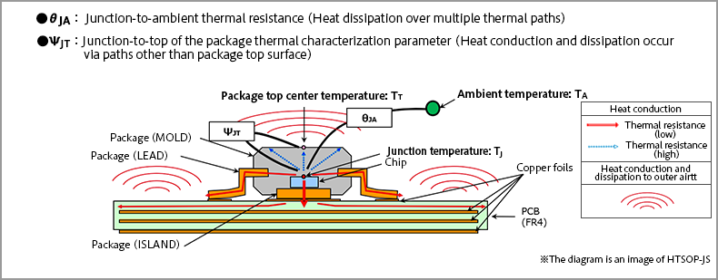
$\Psi_{JB}$ (Junction-to-Board Characterization Parameter): Corresponding conceptually to $\Psi_{JT}$, this is the ratio of the difference between the junction temperature and the temperature of the PCB copper trace 1 mm away from the edge of the chip to the total power consumption of the chip. This parameter can be used to calculate the internal junction temperature of the chip by measuring the temperature of the copper trace at the bottom edge of the chip (in certain scenarios, such as with sensor modules).
In summary, parameters with the $\theta$ symbol (such as $\theta_{JC}$ and $\theta_{JA}$) are not very practical for actual junction temperature calculations. This is mainly because the total heat (total power consumption $P$) generated during chip operation splits into multiple paths: a portion of the heat conducts downward through the pins and solder balls to the PCB copper traces ($P_{board}$), while the remaining heat travels upward through the plastic molding compound into the air or enclosure ($P_{top}$). The problem is that we fundamentally cannot accurately measure what proportion of the power consumption goes upward. Therefore, even if the manufacturer provides a precise $\theta_{JC}$, we cannot accurately calculate the true junction temperature $T_J$.
Ideal Temperature Calculation Theory and Workflow
So, in engineering practice, how do we verify through testing and calculation whether the current design meets the temperature requirements of the project and product?
As mentioned above, the internal junction temperature $T_j$ of the chip is the fundamental standard for evaluating product thermal design. As long as the junction temperature obtained through testing and calculation complies with the junction temperature requirements in the chip datasheet, the product is considered acceptable from a design perspective.
The calculation and evaluation of the chip’s internal junction temperature generally fall into the following three scenarios.
Scenario 1: The chip datasheet provides the temperature parameter $T_c$ at the exact center of the chip package surface. Because the dies inside the vast majority of chips are mounted in the center, the heat-generating core is located directly underneath the center of the package. Heat conducts upward in an inverted funnel shape, meaning the exact center of the package surface is the hottest spot on the entire accessible enclosure.
In this scenario, there is no need to use complex thermal characterization parameters ($\Psi_{JT}$) or back-calculate the junction temperature ($T_j$). We can directly measure the center temperature of the chip surface using a thermocouple and simply compare the test value against the threshold defined in the chip datasheet.
Therefore, when the $T_c$ parameter is provided in the chip datasheet, this is the favorite and most efficient evaluation method for hardware and mechanical engineers in actual work. However, the industry reality is: for the vast majority of consumer-grade or security-grade SoCs and image sensors, their datasheets will almost certainly not provide $T_{c_max}$, but will only provide $T_{j_max}$ or $T_a$.
Scenario 2: During the initial design phase of many complex, large-scale chips, a thermal diode is often etched directly into the heat-generating core area (such as beside the CPU/NPU cluster) for self-protection, enabling measurement of its internal junction temperature.
For example, some master SoCs typically feature an internal TSADC (Temperature Sensor), allowing the core junction temperature to be obtained in real-time directly by software reading registers or sysfs nodes under Linux (e.g., /sys/class/thermal/thermal_zone*/temp). Junction temperatures read in this manner are also the most accurate.
While this method is the most accurate, it is often unfeasible for most low-cost consumer electronics chips, as the vast majority of consumer-grade chips do not have built-in temperature sensors.
When neither of the first two scenarios is achievable, measuring the temperature of the chip’s external surface with a thermocouple and then back-calculating the internal junction temperature using thermal resistance parameters becomes the standard practice and workflow for hardware and thermal design engineers.
The most critical calculation formula for this workflow is:
$$ T_j = T_c + (P \times \Psi_{JT}) $$
Where:
- $T_j$ (Junction Temperature): The target junction temperature we need to calculate.
- $T_c$ (Case Temperature): The center temperature of the surface directly above the chip package.
- $P$ (Power): The current actual operating power consumption of the chip (in Watts).
- $\Psi_{JT}$ (Psi-JT, Junction-to-Top Characterization Parameter): The thermal characterization parameter from the junction to the top of the package (in °C/W).
The laboratory operating steps for the above method are as follows:
- First, measure $T_c$ (the center temperature of the chip surface): It is recommended to use a K-type thermocouple (36 AWG or finer is advised) with high-thermal-conductivity adhesive to securely attach the thermocouple to the exact center of the chip package surface. Next, place the complete device in a temperature and humidity chamber, set the maximum ambient temperature defined by the product PRD for a burn-in test, and once the temperature curve stabilizes, read $T_c$ via a data logger.
- Measure the corresponding dynamic power consumption $P$ of the chip: Under high-temperature environments, semiconductor leakage current increases, leading to higher power consumption. Therefore, nominal power consumption from the datasheet cannot be used directly. Instead, an oscilloscope or high-precision multimeter must be used to measure the actual current and voltage of each sensor power rail (AVDD, DOVDD, DVDD) under high-temperature full-load operation to calculate the true total power consumption $P$.
- Calculate $T_j$ using the formula above: Substitute the measured $T_c$, actual power consumption $P$, and the manufacturer-provided $\Psi_{JT}$ into the formula to accurately derive the internal junction temperature under the current environment.
Taking TI’s 3D ToF Sensor OTP8241 as an example to illustrate the calculation process above, the sensor’s $\Psi_{JT}$ parameter is 6.3 °C/W:
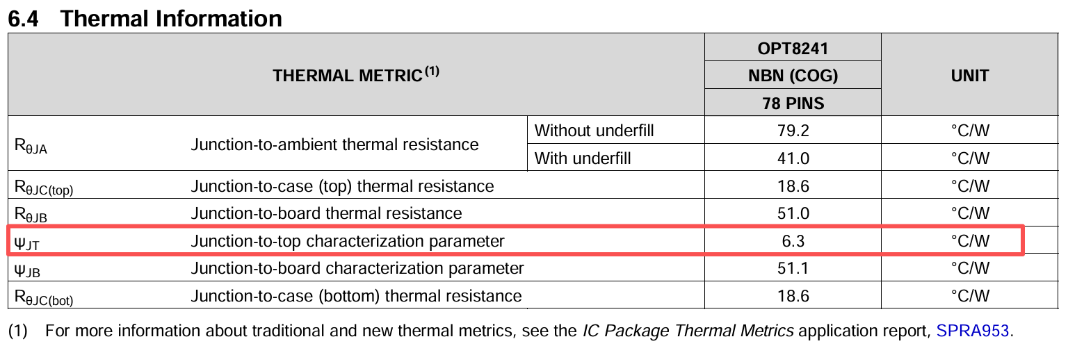
Assuming an extreme burn-in test is conducted in a 70°C chamber, and a thermocouple measures that the temperature $T_c$ at the center of the sensor package surface reaches 85 °C, with an oscilloscope measuring the total power consumption $P$ of all power rails at the current frame rate under full load to be 1.2 W, then the true internal junction temperature undergoing stress is:
$$ T_j = 85 + (1.2 \times 6.3) = 92.56 °C $$
The above outlines the calculation workflow under ideal conditions for relatively accurate testing, estimation, and final evaluation of the thermal design stability and rationality of a product.
However, in real-world product design, for many consumer-grade or security-grade low-cost/low-price SoCs and image sensors, original manufacturers often perform only basic high- and low-temperature operating range tests during R&D finalization (such as calibrating the limit operating junction temperature $T_j$ between -30°C and 85°C) and do not strictly follow JEDEC standards to issue a complete 3D thermal resistance matrix ($\Psi_{JT}$, $\theta_{JA}$, $\theta_{JC}$).
Therefore, in the datasheets of such low-cost consumer chips, the $\Psi_{JT}$ parameter cannot be found at all, making it impossible to precisely calculate the internal junction temperature using the workflow and formula above. In this case, we can only resort to estimation methods to roughly evaluate whether the design is reasonable and meets requirements.
Estimation During Real-World Design
As mentioned above, if the chip datasheet does not provide an accurate $\Psi_{JT}$ parameter, we fundamentally have no way to precisely calculate the junction temperature. In such cases, we can only use empirical estimations to roughly evaluate the rationality and risk factor of the entire product’s thermal design.
In actual product engineering design, the most commonly used method is to use the measurable chip surface temperature $T_c$ to roughly estimate the corresponding junction temperature $T_j$. How to relatively accurately estimate $T_j$ using $T_c$ is closely related to the packaging type adopted by the chip.
FCBGA / Bare Die: These packages are mainly created for high computing power and high heat generation. The silicon die is flip-chipped onto the substrate inside the package, so its heat-generating core directly faces the metal thermal packaging lid on top or is completely exposed. In this scenario, the heat from the chip’s internal PN junction dissipates strictly upward. The empirical value of $\Psi_{JT}$ is 0.1 to 1.0 °C/W, meaning the chip’s internal junction temperature $T_j$ is nearly equal to the surface temperature $T_c$.
QFN / DFN / ePAD-SOIC: These packages feature a bare copper metal pad at the bottom of the chip, which is soldered directly to the PCB ground plane. They are commonly found in Power Management Integrated Circuits (PMICs), motor drivers, and high-power audio amplifiers. Consequently, their heat dissipation direction is strictly downward. However, because the top plastic molding material of this type of package is usually very thin and the physical distance from the silicon die to the top is extremely short, its upward $\Psi_{JT}$ remains very small. The empirical value for $\Psi_{JT}$ is 0.5 to 4.0 °C/W.
QFP / LQFP / TQFP: These packages have gull-wing leads on all four sides, and the black plastic body is relatively large and has a certain thickness. Most conventional MCUs (microcontrollers) and interface control chips (such as USB/Ethernet PHY) typically use this package. Heat dissipates in all directions: part goes downward through the leads, and part dissipates upward through the plastic casing. The empirical value for $\Psi_{JT}$ generally ranges between 2.0 and 8.0 °C/W.
SOIC / TSSOP: These packages have leads on both sides, and the package volume appears relatively thick and heavy compared to the extremely tiny internal die. They are commonly found in conventional logic gate circuits, operational amplifiers, audio ADCs/DACs, or basic low-current analog chips. Heat dissipation occurs primarily through lead conduction. Therefore, for this type of package, the ultra-high thermal resistance of the plastic casing itself acts as an obstruction, causing the surface temperature $T_c$ to be much lower than the internal $T_j$. The empirical value for $\Psi_{JT}$ is generally between 5.0 and 15.0 °C/W. Fortunately, such chips typically have extremely low power consumption (milliwatt level) and generally do not face severe thermal crises.