How PSRAM and LPDDR Reduce Power Consumption
- 29 May, 2026
Due to the inherent self-refresh characteristic of DRAM and the processing of high-frequency communication signals, DDR has always been a major power consumer in electronic system design. This article focuses on summarizing the targeted design strategies implemented by LPDDR and PSRAM to reduce power consumption.
The Power Consumption Issue of DDR
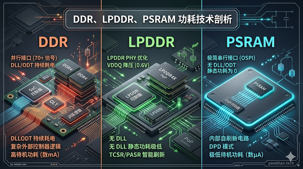
With soaring frequencies, modern DDR (especially DDR5) has long become a major power hog on motherboards. This is why high-end memory modules in our PCs today must wear thick metal heat spreaders, or even be equipped with dedicated Power Management Integrated Circuits (PMICs).
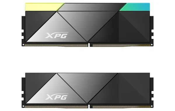
Where does the high power consumption of DDR come from? Generally speaking, the causes of DDR’s high power consumption can be attributed to the following three core parts.
Dynamic Power Consumption
There is a very classic formula for calculating the dynamic power consumption of digital circuits:
$$ P = C \cdot V^2 \cdot f $$
In summary: The dynamic power consumption of a digital circuit is directly proportional to the operating frequency $f$, the square of the voltage $V$, and the parasitic capacitance $C$.
Modern DDR4 easily reaches 3200 MT/s, and DDR5 even surges to 5600 MT/s or higher, meaning its internal base frequency is as high as 2.8 GHz or more. At such high frequencies, hundreds of millions of transistors inside the chip and dozens of external data and clock lines must toggle their voltage levels (from 0 to 1 / from 1 to 0) billions of times per second. This high-frequency switching action generates huge instantaneous currents and is also the largest heat source for DDR in its active state.
Similarly, PCB traces and connectors on the circuit board introduce a certain amount of parasitic capacitance (corresponding to $C$ in the dynamic power consumption formula above). Furthermore, to ensure that signals remain precise when routed and branched across the PCB, DDR4 must maintain a relatively high I/O driving voltage of $1.2\text{V}$ ($1.1\text{V}$ for DDR5). According to the dynamic power consumption formula above, its power consumption is exponentially amplified.
Static Analog Dissipation
When frequencies enter the microwave level (such as the base frequency of DDR5600 mentioned above), DDR must attach power-hungry advanced analog circuits to its peripheral interface modules (i.e., the DDR PHY module) to prevent high-frequency communication signals from distorting:
- DLL (Delay-Locked Loop): To ensure that external clocks and internal data are precisely aligned within a nanosecond or even picosecond window, the DLL module must run at high speed in the background, constantly detecting and forcibly compensating for tiny physical delays. As long as the clock keeps running, the power consumption of the DLL will not stop, which is one of the sources of static base current.
- ODT (On-Die Termination): High-frequency signals generate severe electromagnetic reflections on long PCB traces. To absorb these reflected waves, DDR instantaneously turns on internal ODT resistors when receiving data. This is equivalent to laying a DC path in the circuit, where signals are directly dissipated as heat, turning into actual thermal loss.
For the working principles related to DLL and ODT, you can refer to the article Can PSRAM Be a Solution to DDR Shortages?.
DRAM Self-Refresh Power Consumption
Fundamentally, the underlying layer of DDR is a DRAM storage array, where every single bit of data relies on the charge in a miniature capacitor to be maintained.
In reality, capacitors inevitably leak charge. To prevent data loss, even when the system is completely idle (without any read/write operations), the SoC master controller must send a self-refresh command to the DDR every few milliseconds, forcing billions of capacitors inside the chip to be frequently charged and discharged.
This large-scale charge and discharge working mechanism means that even during standby and sleep, DDR cannot achieve true zero power consumption like static logic circuits.
For the specific working principles of DRAM, you can also refer to the article Can PSRAM Be a Solution to DDR Shortages?.
How LPDDR Mitigates Power Consumption Issues?
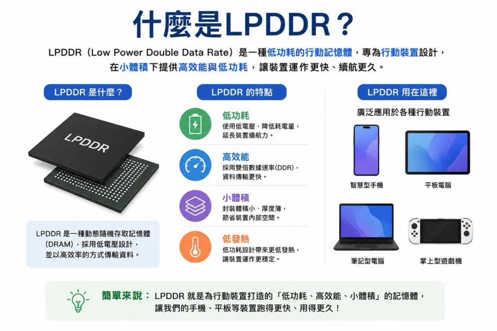
To address the high power consumption issues of DDR mentioned above, LPDDR prioritizes low-power design in its architecture. It has carried out targeted renovations on the underlying physical architecture of standard DDR. While maintaining a high data throughput rate, it drastically reduces power consumption, making it more suitable for mobile high-performance computing devices such as laptops and smartphones.
Targeting Dynamic Power Consumption
Still referring to the formula for digital circuit dynamic power consumption: $P \propto C \cdot V^2 \cdot f$.
To reduce power consumption while maintaining high frequency ($f$), the first step is to focus on the I/O interface voltage ($V$).
As mentioned above, the core and I/O voltages of standard DDR4 are typically both 1.2V. In contrast, LPDDR4X directly lowers the I/O voltage responsible for external communication (VDDQ) to 0.6V. $0.6^2$ is only one-quarter of $1.2^2$. This means that simply in terms of high and low voltage level transitions on the data bus, LPDDR4X saves 75% of dynamic power consumption compared to DDR4.
In addition, to ensure signal integrity at such low voltages, LPDDR adopts a dedicated Low-Voltage Swing Terminated Logic (LVSTL) and requires the physical distance between the master controller and the memory to be extremely short (usually using PoP stacked packaging or compact SiP), which also helps reduce the parasitic capacitance $C$ of the PCB traces.
Targeting Static Power Consumption
As mentioned above, to align clock signals in high-frequency communications, DDR adds a dedicated DLL module. This module runs continuously even when the system is under no load and consumes extreme amounts of power.
Therefore, LPDDR completely abandons the internal DLL module in its chip design. Instead, to solve the clock signal alignment problem, it requires the memory controller of the master SoC to execute extremely complex Training algorithms during system boot, allowing the SoC’s LPDDR controller to measure the delay of each data line and then perform active phase compensation inside the SoC.
This transfers the burden of signal synchronization to the SoC master, allowing LPDDR to shed its biggest static power consumption burden.
Introducing TCSR and PASR Mechanisms
For the self-refresh actions performed on its internal DRAM array, standard DDR makes no distinctions. Regardless of whether the current temperature is high or low and whether the data is in use, it refreshes all bits across the entire array at the highest frequency, which actually results in a huge waste of power.
Therefore, LPDDR integrates two intelligent refresh control mechanisms internally to optimize power consumption:
- TCSR (Temperature Compensated Self Refresh): There is a temperature sensor inside the chip. When it senses that the device is in a cold state (where capacitor leakage is relatively slow in this state), it automatically lowers the self-refresh frequency.
- PASR (Partial Array Self Refresh): For sleep scenarios, before the system enters sleep, the operating system uses special commands to tell LPDDR which banks are empty. This way, during sleep, LPDDR can directly power down the empty banks during self-refresh, only maintaining self-refresh for banks containing data.
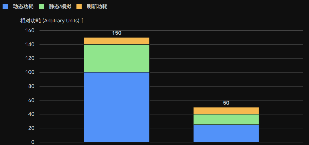
Through the targeted power consumption optimization design across these three dimensions, the power consumption of LPDDR is significantly reduced compared to DDR:
How PSRAM Solves Power Consumption Issues
Although, as summarized in the article Can PSRAM Be a Solution to DDR Shortages?, PSRAM and DDR/LPDDR are actually products targeting completely different fields and applications, PSRAM’s low-power performance is indeed prominent. Therefore, this section also summarizes the efforts made by PSRAM in reducing power consumption.
If LPDDR achieves relatively low power consumption while guaranteeing performance through extremely expensive advanced manufacturing processes and extremely complex fine-grained management, then the logic behind PSRAM solving power consumption issues is essentially “letting go” (Zen style)—that is, trading extreme power savings for raw physical simplification and architectural reduction (of course, its performance is completely out of class compared to DDR/LPDDR).
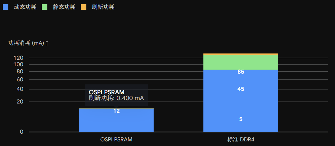
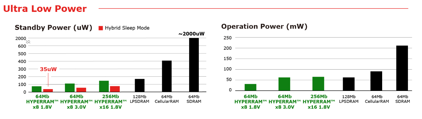
The figure below shows the power consumption profile of a Winbond PSRAM:
Targeting Dynamic Power Consumption
Analysis is still based on the digital circuit dynamic power consumption formula: $P = C \cdot V^2 \cdot f$.
For dynamic power optimization, LPDDR’s approach is to lower the voltage ($V$) as much as possible, which also requires the distance between the SoC master and LPDDR to be minimized. In contrast, PSRAM’s approach is to minimize the frequency ($f$) and pin capacitance ($C$).
- Serial Bus: DDR typically has 60 to 100 I/O pins, and the massive routing network on the motherboard leads to large parasitic capacitance ($C$). In contrast, mainstream OSPI PSRAM has only 8 data lines and fewer than 12 pins in total.
- Low Frequency Band: The physical clock of DDR is generally in the microwave band above 1200 MHz. PSRAM proactively avoids the complexity brought by microwave communication by capping the maximum clock well within 200 MHz.
As a result, due to fewer pins and lower frequencies, the physical capacitance and number of toggles that the master SoC and PSRAM need to overcome during data communication are reduced by orders of magnitude. Therefore, even though PSRAM’s I/O voltage still adopts the conventional 1.8V (without dropping to 0.6V like LPDDR, thus lowering PCB layout and routing requirements), its overall dynamic power consumption remains far lower than that of DDR.
Targeting Static Analog Dissipation
Since the clock frequency is below 200 MHz, there is no need to deal with high-frequency communication signal issues, no need for a DLL to forcibly align nanosecond-level phases, and no need for ODT to absorb electromagnetic reflections of high-frequency signals. Consequently, the DLL and ODT modules, which have high static power consumption in DDR, can be eliminated.
When there are no read or write operations, the interface terminals of PSRAM can enter absolute silence, and static power consumption can be directly reduced to zero.
Targeting Sleep Base Current
Whether it is DDR or LPDDR, even when the system enters a sleep state, the SoC’s DDR controller must remain operational to refresh the internal storage arrays of DDR/LPDDR (LPDDR can only turn off refresh for some idle banks). This causes the sleep base current of DDR/LPDDR to remain stubbornly high even during sleep.
To address this pain point where DDR must be externally managed by the SoC, PSRAM uses a completely different self-refresh and sleep control logic, completely resolving the base current issue during sleep. This exact feature is why PSRAM is well-suited for applications that are extremely sensitive to sleep power consumption.
PSRAM features an internal self-refresh module. Thus, when the device enters a sleep state, the master SoC can directly cut off the external clock and completely power down. The extremely power-efficient micro-RC oscillator inside PSRAM wakes up and recharges the capacitor array at a very slow pace to maintain data persistence.
Through the targeted power consumption optimization above, there is a massive order-of-magnitude difference in power consumption between DDR and PSRAM:
Under Full-Load Active State:
- Standard DDR4: Consumes anywhere from 2 watts to 3 watts, with currents at the level of hundreds of milliamperes (mA), causing noticeable heat on the chip surface.
- OSPI PSRAM: When streaming data at 200 MHz, the current is typically only around 20 mA to 35 mA.
Under Deep Sleep State:
- Standard DDR4: Even upon entering sleep, its base current typically remains as high as 10 mA to 20 mA, which is also the primary reason why AOV Camera power consumption stays high.
- OSPI PSRAM: Standby current drops off a cliff, typically ranging between 20 µA and 50 µA.