Can PSRAM Become the Solution to DDR Shortages?
- 27 May, 2026
With the current tight supply and drastic price fluctuations in the DDR memory market, some SoC vendors in the IPC field have started promoting Camera SoC platforms with built-in PSRAM. What are the differences between PSRAM and the DDR we commonly use, and what applications are they suitable for? This article attempts to clearly answer these questions.
To understand what PSRAM actually is, we must first understand the difference between SRAM and DDR (DRAM).
SRAM vs. DRAM
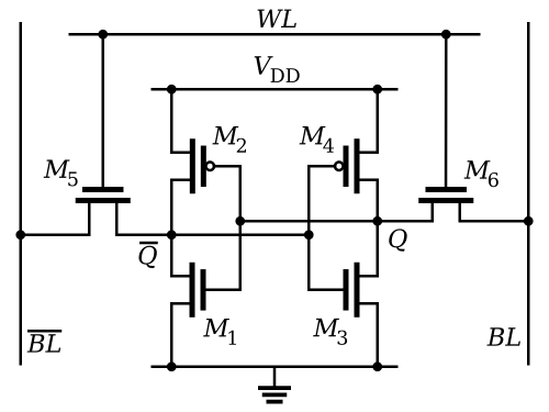
SRAM can be considered the high-end, wealthy elite of the storage world, with the most common current use being the L1/L2 Cache inside CPUs. Storing 1 bit of data requires a full 6 transistors (the 6T architecture). These 6 transistors are cross-coupled to form a logical closed-loop (a flip-flop).
With this storage structure, accessing bit information is extremely simple and reliable:
- Writing data: A high external voltage is applied to forcefully set the state of the flip-flop to one side.
- Reading data: The state across the two ends of the flip-flop is measured directly. This read operation is non-destructive to the original state of the flip-flop, and the speed is extremely fast (nanosecond or even picosecond level).
Its advantages are that this storage structure is extremely stable, the state is locked forever as long as power is maintained (no refreshing required), and reading a memory bit is non-destructive with blazing speed.
However, the disadvantages are certainly that the footprint is too large, it is difficult to scale up the capacity, and the cost is extremely high.
The figure below shows the circuit structure of a single storage bit in SRAM:
The initial birth and subsequent continuous evolution of DRAM were both aimed at solving the aforementioned issues of large capacity and low cost.
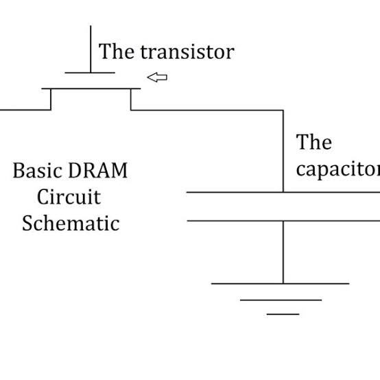
In the design of a single-bit DRAM storage cell, only 1 transistor + 1 miniature capacitor are used. An analogy for this storage structure is: the transistor is a water faucet, and the capacitor is a small bucket. A full bucket represents 1, and an empty one represents 0.
This bit storage structure has a fatal physical flaw: the capacitor leaks electricity. Therefore, within a few milliseconds, a full bucket leaks down to a half-full bucket, and eventually, 1 becomes 0. Thus, to maintain the stability of the bit state, the transistor must be periodically opened to check (determine whether it is 0 or 1), and if it is 1, the water (charge inside the capacitor) must be refilled. This is the physical essence of why DRAM requires dynamic refreshing.
Worse yet, the read and write process for each bit in DRAM is extremely complex:
- Writing data: First, open the transistor (faucet) and pump charge into the capacitor (bucket) to represent 1, or drain the charge to represent 0.
- The DRAM read process is a complex, destructive read operation: First, you must detect whether there is water (charge) in the bucket. To detect this, you can only open the transistor and let the water flow out to the external bus (Bitline). An external Sense Amplifier senses the weak water flow and determines whether the previous state of the bit was 0 or 1. Because the water flows out during a read operation, the original data state is destroyed after reading. Therefore, at the end of every read operation, DDR must forcibly execute a write-back action to refill the bucket with the 1 that was just read.
The above is a brief summary of the working principles of SRAM and DRAM. DDR, LPDDR, and PSRAM, which will be introduced later, are all based on DRAM; their internal bit storage array structures and read/write processes follow the DRAM conditions described above.
💡 Note: PSRAM is not SRAM, but rather DRAM. The reason it carries a “P (Pseudo)” is because it is a misnomer. Its internal structure is still DRAM that leaks electricity, except that a micro-controller is integrated inside the silicon chip to automatically handle the refresh operation, masquerading to the external host controller as SRAM that requires no refreshing.
To understand how PSRAM actually works, a good starting point is to understand how the most commonly used DDR works, and then examine the differences between it and DDR.
What Exactly is the Technical Barrier of DDR?
Note that while the internal structures and workflows of different DDR specification versions—as well as their earlier predecessors like SDR—are extremely complex, the purpose of this article is primarily to clearly explain the differences in workflow and structure between DDR/LPDDR and PSRAM. Therefore, detailed minor points will not be summarized; only the parts with distinct differences from PSRAM will be covered.
In product design, when using external DDR, we often face issues such as high DDR power consumption and complex circuit design. Because of this, mainstream Camera SoC manufacturers generally integrate DDR internally to reduce system design and debugging difficulty. The primary reason for this complexity in DDR is its pursuit of high throughputs reaching tens of GB/s.
The figure below is a typical connection diagram between an SoC DDR controller and a DDR chip:
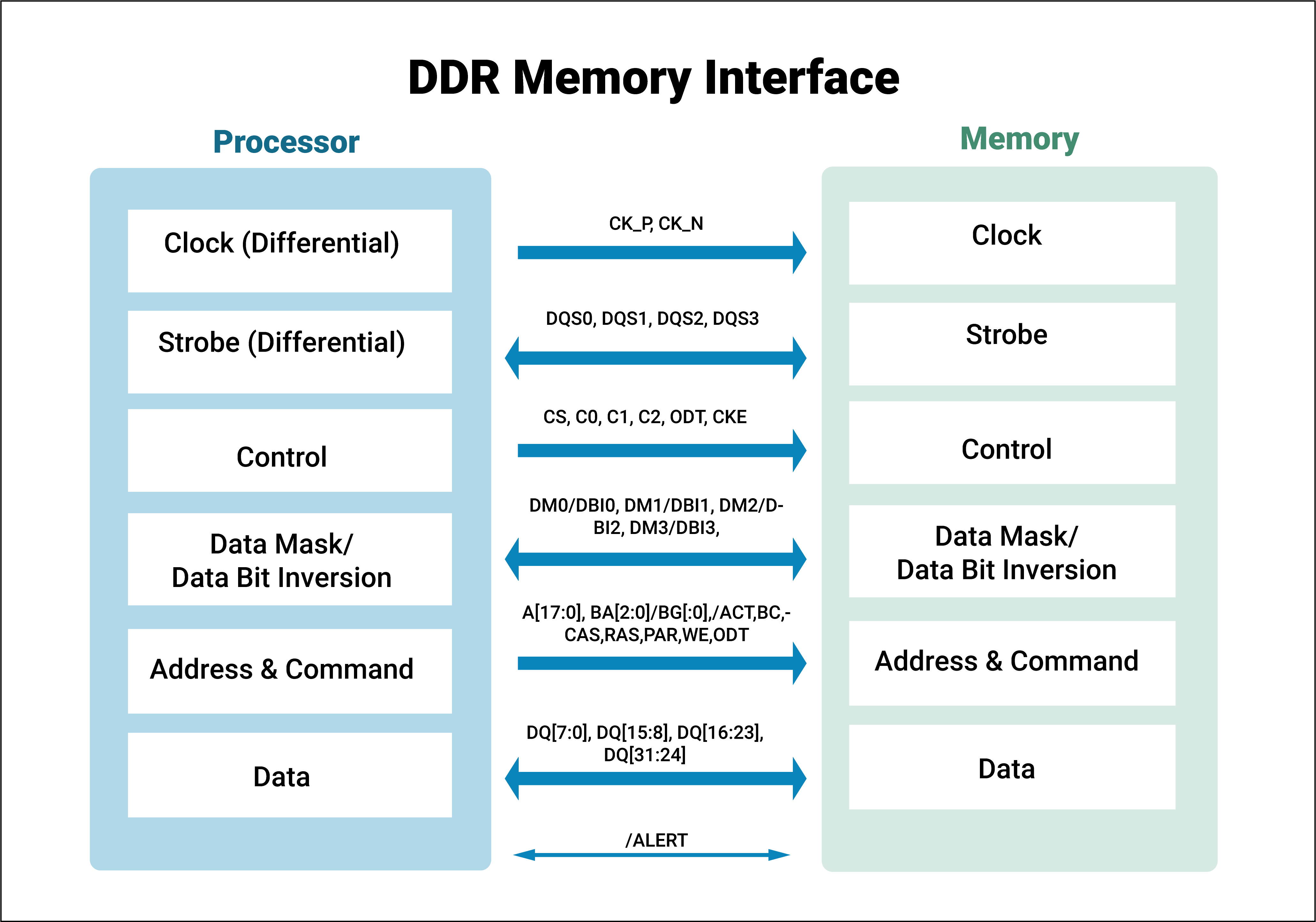
To pursue extremely high throughput between the SoC and DDR, current mainstream DDR5 has achieved 5600 MT/s (Mega Transfers per second) or even higher.
The basic principle of DDR (Double Data Rate) communication is: transmitting data on both the rising edge and the falling edge of the clock signal. Therefore, when a DDR5 data throughput reaches 5600 MT/s, its actual physical clock (i.e., the true square-wave oscillation frequency sent by the SoC to the DDR via the CLK pin) reaches 5600 / 2 = 2800 MHz (2.8 GHz)!
A fundamental frequency of 2.8 GHz already falls into the typical microwave frequency band on a PCB. At this frequency, the copper traces on the motherboard are no longer simple wires, but rather microstrip antennas. Issues caused by these antennas, such as signal reflection, crosstalk, and attenuation, become extremely severe. This is the core problem that high-frequency DDR must solve. The high-speed analog and mixed-signal design capabilities required to solve this problem are what truly separate mid-to-low-end memory manufacturers from international giants (such as Samsung, SK Hynix, and Micron).
To solve the aforementioned high-frequency signal issues, high-frequency DDR adopts DDL (Delay-Locked Loop) and ODT (On-Die Termination) solutions in its signal design.
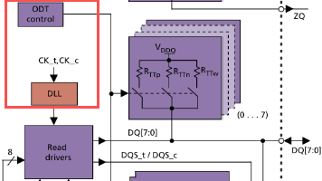
The purpose of the DLL (Delay-Locked Loop) module is primarily to combat internal clock delay within the DDR chip.
During communication when the external SoC accesses data in DDR, the clock signal travels through the PCB traces, arrives at the DDR pins, and must pass through a complex internal routing tree inside the DDR to reach the registers that finally output data. This physical path generates an internal propagation delay of about 0.1 to 0.2 nanoseconds.
Without a DLL, by the time DDR data reaches the SoC pins, it might be delayed by half or even a full clock cycle. The external SoC expects to receive data precisely on the clock edge, and such access would result in reading completely garbled data.
The role of the DLL module is like an extremely precise timing predictor. During operation, it continuously measures the inherent physical delay between the arrival of the external clock and the emission of internal data. Then, through an internal voltage-controlled delay line, it intentionally advances the clock used to trigger data inside the DDR, ensuring that the data returned by the DDR appears at its pins precisely aligned with the SoC’s clock.**
The purpose of ODT (On-Die Termination) is mainly to eliminate signal echoes.
As mentioned above, when the signal frequency of a transmission line reaches the GHz level, the copper wires on the PCB are no longer simple conductors, but rather transmission lines. When the SoC transmits data (electromagnetic waves) to the DDR at full speed, if the signal hits the end of the DDR pins and finds an impedance mismatch, the electromagnetic wave will bounce back along the same path, creating an echo signal. This echo signal will collide with the next new wave being sent by the SoC, causing the waveform across the entire bus to degrade (professionally termed ringing, overshoot, or undershoot), resulting in instantaneous, massive data corruption.
To cope with echo issues caused by impedance mismatches in RF signals, the JEDEC specification dictates adding termination resistors on the silicon inside the DDR chip (On-Die) to absorb reflected waves—this is ODT.
Structure and Internal Characteristics of PSRAM
Compared to the complexity faced by high-speed DDR in high-frequency signal communication, the structure of PSRAM is much simpler.
The external communication frequency of the vast majority of PSRAM is typically limited to within 200 MHz, avoiding severe electromagnetic reflections and nanosecond-level clock skew issues. Consequently, its physical interface becomes conventional CMOS/LVCMOS transceivers.
Current mainstream PSRAM and master SoCs communicate via QSPI (4 data lines) and OSPI (8 data lines) interfaces. The SoC simply sends simple SPI serial commands, and PSRAM translates these simple commands internally into the complex instruction combinations required by the underlying DRAM array (such as splitting them into Active row activation -> Read/Write column access -> Precharge). As a result, the SoC no longer needs to integrate a complex DDR controller.
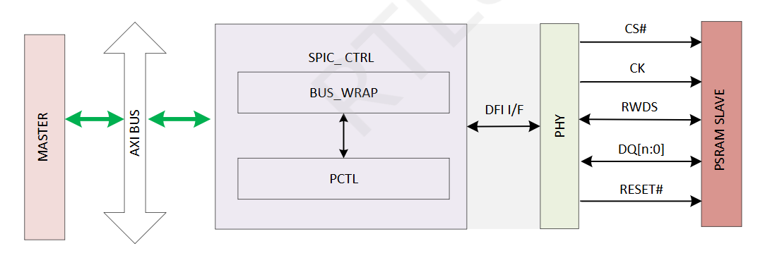
Compared to DDR, a major innovation of PSRAM is its built-in self-refresh counter. PSRAM uses this internal self-refresh counter to completely take over the self-refresh behavior of its internal DRAM array. In this case, when entering sleep mode, the master SoC can even truly shut down (as long as power to the PSRAM itself is maintained) without affecting the data inside the PSRAM. Thus, power consumption in sleep mode is drastically reduced.
- In contrast, with DDR, even when the host goes to sleep, the SoC’s memory controller cannot be powered off; it must continue to maintain specific voltage levels on the clock pin or CKE (Clock Enable) pin. This causes a portion of the power domain inside the SoC to remain unclosable, making it very difficult to reduce the overall baseline current of the system.
Overall, therefore, the design philosophy of PSRAM is to sacrifice extreme throughput and capacity (since communication throughput is too low, high capacity is meaningless, which is why current mainstream PSRAM capacities typically range from 32 Mb to 256 Mb). By adding a large amount of logic circuitry inside the chip to solve the DRAM array leakage problem and presenting an extremely user-friendly interface to the master SoC, it ultimately trades for extreme power savings and minimalist hardware design.
Conclusion
Generally speaking, although the manufacturing of the internal storage core array (DRAM Cell) of DRAM still requires extremely advanced process nodes, this is not an insurmountable hurdle. The true technical barrier in the DDR domain lies in high-speed analog and mixed-signal design capabilities (namely peripheral circuits including the DLL, ODT, and high-speed PHY interfaces briefly outlined above).
For many manufacturers producing PSRAM or older legacy DDR specifications (such as DDR2 or low-speed DDR3), their strengths lie in digital logic design and low-power control. In the 100 MHz to 200 MHz frequency band, digital signals remain relatively ideal square waves, eliminating the need for overly complex analog circuits to repair signals.
However, once they want to advance toward high-speed DDR4 or even DDR5, manufacturers must assemble top-tier analog circuit design teams. What they must solve are no longer simple 0-and-1 logic problems, but microwave-level electromagnetic field problems. In addition to the aforementioned DLL and ODT, modern high-speed DDR must also integrate advanced analog anti-interference technologies such as VREF (Internal Reference Voltage Calibration) and even DFE (Decision Feedback Equalizer), which were previously found only in high-end communication chips (like PCIe and Ethernet PHYs).
This is why there are countless manufacturers in the market capable of making PSRAM, while those capable of stably supplying high-speed LPDDR4X and DDR5 can be counted on one hand. The essence of the latter is an ultra-high-speed RF/analog chip disguised in memory clothing.
Therefore, combining the internal architectural composition and working logic of DDR and PSRAM discussed above, it is clear that these two fundamentally target completely different application domains and are not comparable.
- The core mission of the DDR series (including LPDDR commonly used in mobile devices) is to provide extreme memory bandwidth. As long as the system runs a massive operating system (such as standard Linux, Android, Windows) or needs to process intensive matrix operations and high-definition multimedia streams, it must be handled by DDR.
- The purpose of PSRAM is to provide the host controller with a cache much larger than on-chip SRAM, all within limited PCB space and with extremely low standby power consumption. As long as the device is purely battery-powered (low-power), processes audio, acts as a low-resolution smart doorbell, or is a lightweight IoT device with a screen, using PSRAM is very appropriate—provided, of course, that the software architecture transitions from heavy Linux to an RTOS, or significantly optimizes application-layer memory footprints and bus overhead.