Summary of Learning on RF Circuit Components
- 20 Jan, 2025
This note provides a brief summary of the basic working principles and applications of various common component circuits in wireless radio frequency (RF) circuits, laying a solid foundation for understanding and designing complete RF circuit system architectures in the future.
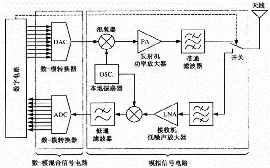
The figure below shows a typical and simple block diagram of an RF system:
The various primary components used in wireless RF circuits can be categorized into two main classes—active components and passive components—based on whether they require an external power supply.
- Active components include: RF Transceiver, Power Amplifier (PA), Low Noise Amplifier (LNA), Radio Frequency Front-End Module (FEM), active crystal oscillator, RF switch, etc.
- Passive components include: Filter, Duplexer, Diplexer, Coupler, resistors, capacitors, inductors, antenna, passive crystal oscillator, etc.
RF Transceiver
An RF Transceiver actually encompasses an RF Transmitter and an RF Receiver, meaning it possesses both RF signal reception and transmission capabilities. The RF Transceiver is the core of the entire RF circuit system, used to generate high-frequency RF signals suitable for wireless communication. The so-called RF system architecture is essentially centered around the RF Transceiver chip, complemented by other peripheral RF front-end circuits.
The main functions of an RF Transceiver are:
- For RF signal transmission: Up-converting and frequency-synthesizing the baseband modulated signal, performing preliminary signal amplification to generate the RF signal, which is then further amplified by the PA, switched via the antenna switch, and radiated out through the antenna.
- For RF signal reception: The RF signal received from the antenna passes through the antenna switch, is amplified by the LNA, and is then fed into the RF transceiver chip for down-conversion and filtering operations to recover the baseband modulated signal, yielding the baseband demodulated signal.
Therefore, in a strict sense, the RF Transceiver is separate from the PA, LNA, and RF switch, each having its own distinct functions. However, integration in consumer electronics is becoming increasingly high today. Many RF transceiver chips actually integrate the PA, LNA, and RF switches inside them. In some 5G smartphone RF transceiver solutions, even the antenna is integrated, making the design and debugging of RF circuits very straightforward.
Power Amplifier (PA)
PA stands for Power Amplifier. In RF circuits, the role of the PA in the RF transmission chain is to amplify the power of the RF signal generated by the RF Transceiver so that the power radiated through the antenna meets the transmission distance requirements.
From the perspective of manufacturing processes, there are currently four main processes commonly used for PAs: Gallium Arsenide (GaAs), Gallium Nitride (GaN), Silicon Germanium (SiGe), and CMOS. Among them, the GaAs process occupies a mainstream position in the field of RF power amplifiers.
In specific product applications, it is necessary to fully recognize the importance of reducing PA power consumption. This is because PA power consumption accounts for the majority of the total RF circuit power consumption. Product requirements for multi-antenna and high communication rates mean that PA power consumption significantly impacts the overall device power consumption, battery life, and thermal design.
Low Noise Amplifier (LNA)
LNA stands for Low Noise Amplifier. The function of an LNA is similar to that of a PA in that both amplify RF signals. However, the PA is used in the transmission chain to provide power amplification for the RF signal to be transmitted via the antenna, ensuring that signal transmission meets distance requirements. In contrast, the LNA is used in the reception chain to amplify the RF signal received from the antenna (which is typically very weak) to meet the requirements of RF signal demodulation.
Because the RF signal received from the antenna is generally extremely weak, the noise generated by the operation of the amplifier itself can cause severe interference to this weak signal. The “low noise” in LNA refers to the fact that the LNA amplifier itself has an extremely low noise figure (this is the most characteristic feature of an LNA; the lower the noise, the higher the sensitivity). This allows it to maximize sensitivity and signal-to-noise ratio (SNR) while amplifying the received RF signal, thereby helping the demodulation circuit successfully extract the baseband signal.
Radio Frequency Front-End Module (FEM)
FEM stands for Front-End Module. An FEM is essentially a module that integrates multiple RF unit circuits into a single chip. For example, an FEM may integrate a PA, LNA, filters, RF switches, etc., and some modules even include the RF transceiver and antenna array. The existence of FEMs is primarily driven by the demands for higher integration and lightweight product design, while also reducing the complexity and difficulty of RF debugging and development.
Because an FEM is simply an integrated module of multiple RF circuit units, its overall functionality and performance metrics are determined by the internal RF unit circuits it contains.
RF Switch
An RF switch is essentially a switch that can be used to determine and control the time-shared connection of TX and RX to the antenna at the same frequency point, or to control when systems of different frequency bands are connected in the RF chain. Therefore, from a logical perspective, this component can be considered an ideal switching device, typically referred to as an RF switch in RF circuits, or an antenna switch if used to control the connection and switching of antenna ports.
Of course, unlike ordinary switches, an RF switch operates in the high-frequency RF domain and therefore possesses unique operating parameters: operating frequency (the allowable frequency range suitable for the switching device), isolation between ports (the degree of isolation between multiple channels controlled by the switch to avoid mutual interference as much as possible), and insertion loss (the loss of signal power caused by inserting the switching device, which should ideally be as low as possible), etc.
Diplexer / Duplexer
This has already been explained in great detail in the article [[Correction on the Understanding of Dual-Frequency WiFi Antenna Reuse and Comparison between Duplexer and Diplexer]].
Filter
The application of filters in RF circuits and systems covers both transmission and reception aspects:
- In reception, the main purpose is to maximize the attenuation of unwanted out-of-band signals contained within the received signal while minimizing any impact on the signals in the desired frequency band.
- In transmission, they are used to minimize and attenuate harmonics, spurious emissions, and out-of-band leakage present in the transmitter circuit, thereby avoiding co-existence interference with communications in various RF bands.
The specific implementation principle of a filter is a two-port network formed by R, L, and C resonant circuits. It utilizes the frequency-selective characteristics of the resonant circuit to provide matched transmission for frequency signals within the passband, while causing mismatch and attenuation for frequency signals within the stopband, thereby achieving signal spectrum filtering.
Based on their filtering characteristics across signal frequency bands, filters can be categorized into low-pass filters, high-pass filters, band-pass filters, and band-stop filters.
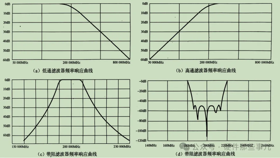
Based on the types of components used to implement the filter, they can be classified into active filters and passive filters. The filters used in consumer electronics are generally passive filters.
Power Coupler
A power coupler is a passive component that taps off a portion of the signal power and energy from the RF path through coupling in an RF circuit. This coupled energy is then used to detect and perform feedback adjustment on the output power of the RF path. Based on its working principle, a power coupler is typically used in the transmission path. The most typical application scenario is coupling a portion of the energy from the output circuit of the power amplifier (PA), detecting this energy, and using a feedback mechanism to control the output power level of the power amplifier. Therefore, with increasing integration levels, most PAs now integrate power couplers internally to feedback and control their transmission power, and standalone external couplers are only required in very specialized applications.
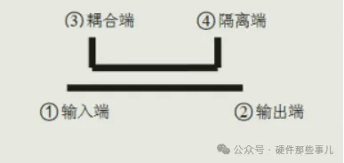
The figure below shows the equivalent circuit diagram of a power coupler. It is generally a four-port passive component, where the power output from the PA is connected via input port 1 and output via output port 2. Aside from the energy output through output port 2, a portion of the energy is coupled out at coupling port 3. By feeding the energy from this coupling port into the RF transceiver chip, it can be used to detect the output power of the power amplifier, which is then adjusted and controlled. Output port 4 is an isolated port with no power output.
References
- Wireless Cheatsheet: Introduction to RF Circuit Design, Chapter 6
- RF - Filter Basics
- RF - Directional Coupler Basics